Towards the fabrication of silicon devices with ultrasmall mode volumes using sub-nanometre-sized dielectric bowtie cavities
Recent developments have brought miniaturization to the centre stage also in photonics because it is required for realizing dielectric bowtie cavities5 with ultrasmall mode volumes—a regime previously believed to be accessible only in plasmonics19,20. In 2005, there were predictions that the existence of low mode volumes had been predicted but not proven until just recently, because realistic designs were missing and the experimental progress was hindered by the extreme requirements on the fabrication. Dielectric bowtie cavities harness the field discontinuities at material boundaries to strongly confine light inside dielectrics22,23, and hold the promise of unprecedented light–matter interaction strengths, fostering new developments in nanolasers and optical interconnects24, nonlinear photonics25, all-optical switching26, cavity quantum electrodynamics7 and cavity optomechanics27. The width of the bowtie is the most crucial parameter because it determines the field enhancement22. The first experiment5 demonstrating confinement of light below the diffraction limit in dielectric bowtie cavities employed 8 nm wide silicon bridges with an aspect ratio of 30, and although minor improvements along this route may be possible, it appears futile to try to scale conventional lithography and etching to atomic dimensions with aspect ratios exceeding 100. The use of voids and low-refractive-index features with extreme aspect ratios are particularly challenging to fabricate because they are needed in some of the most radical applications ofnanocavities. The resolution limit of around 50 atoms has been preventing development of top-down fabrication, which allows for precise edge position with both accuracy anddisorder at the level of a single Silicon atom.
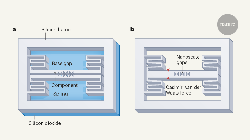
Here we propose and demonstrate a new approach to the manufacturing of semiconductor devices. It is possible to build devices with unprecedented dimensions by using the ubiquitous surface forces that act on objects separated by a few tens of nanometres. Our experiments use these forces to enable controlled and determinative collapses to make smaller, sub-nanometre-sized devices.
A bottom up approach is used where structures are self-assembled using effects such as van der Waals or hydrogen-bonding forces, when fabrication of functional materials and devices at the micro- and nanoscale. The bottom-up approach has enabled research on a wide range of devices with near-atomic dimensions. Such miniaturization is crucial for a wealth of research and technology that rely on an increased surface-to-volume ratio, strong field gradients or quantum effects. The miniaturization of semiconductor technology has slowed, and the industry forecasts no laterallithography features below 8 nm until 2037. At the same time, while bottom-up approaches can achieve feature sizes down to atomic scales, synthetic self-assembly remains far from capable of replicating the hierarchical and scalable self-assembly in biological systems13. A practical consequence is that a wealth of research on bottom-up nanotechnology for information technology always had to rely on top-down technology for the interconnect architecture. For example, lithographically defined wires or waveguides are needed to contact single-molecule devices14 or single-quantum-dot devices7. Combining the scalability of top-down planar technology with the resolution of bottom-up approaches would open vast perspectives15, but they are commonly considered disjoint. Self-assembly has been explored for fabricating origami-like structures in microelectromechanical systems16, which enable unique geometries but not nanoscale dimensions. Strategies for combining nanoscale self-assembly with planar technology are therefore scarce17,18, and a pathway for their direct integration was so far missing.